

Published on Sep 05, 2023
This Project includes the study of the processes involved in VLSI design. Analog properties of the circuit have been considered through out this project. Sense amplifier is an essential circuit in a RAM.
The purpose of the whole circuit is to sense the low swing signal and read it from the RAM cells. The report explains how the design is done based on the new technology models 65 and 45 nm technologies.
A differential voltage sense amplifier has been considered here. Practically there might be some changes based on the model files received from the foundry.
Designed circuit is analyzed and then fine tuned looking in to the output as per the requirement. It is basically a trade of between power consumption and the frequency of operation etc.
Once the schematic or the circuit diagram is frozen, the layout has been done in different method and compared the performance.
Through out this project I have used LT Spice for the simulation of the circuitry and Microwind Lite for the layout and performance comparison. These tools are freely available.
A sense amplifier is an active circuit that reduces the time of propagation from an accessed memory cell to the logic circuit located at the periphery of the memory cell array, and converts the arbitrary logic levels occurring in a bit line to the digital logic level of the peripheral.
Layout area restrictions are specific to the memory design. In memories sense amplifier layout should fit either in the bit line pitch when each bit line requires individual data sensing or in the decoder pitch when a multiplicity of bit lines are connected to a single sense amplifier.
Sense amplifiers are classified by circuit types such as differential and non differential, and by operation modes such as voltage, current and charge sense amplifiers.
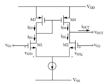
A sense amplifier is nothing but a differential voltage amplifier with a current mirror load.

In the figure there is a current sink ISS which is a constant current sink. The current through this would be always constant and hence the Sum of iD1 and iD2 would be always constant. To keep ISS constant in this circuit, if there is a decrease in one of the branch current the other branch current increases.
Here in this circuit the load is a current mirror. The current mirror circuit consists of transistors M3 and M4. When a differential input is applied (bit and bit' lines), let's assume the higher voltage is applied to the transistor M1 gate and the compliment is on the M2 gate. In this case the current through M1, that is iD1 increases and the current iD2 decreases. Since iD1=iD3 the current mirror draws the same current as iD1, which results in a mirrored current iD4 = iD3 = iD1.
It can be observed that the current iD4 increases where as the iD2 decreases. Also notice that ISS needs to be constant and hence when ever iD2 decreases iD1 will increase and iD4 too increases. If the increase in iD1 is ?I then the decrease in iD2 will also be ?I.
At the output it can be observed that there is a difference of 2?I in current. The excess 2?I will be sunk by the output. This means if a ?I current difference is there at the input there would be a 2?I current flowing through the output. Thus the voltage difference is transferred in to a current difference and this current is amplified at the output and again this is converted as a voltage at the output.
The ISS keeps the current always constant and because of this it brings one of the transistors to higher saturation by drawing more current through that branch when the other branch supplies reduced current.